|
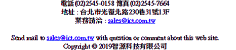
V-by-One® HS IP core |
|
V-by-One® HS IP
core
V-by-One®HS是經由Thine Electronics
Inc. 發展而成支援更高速以及更高度被更好的FPD技術所需求的解決方案,同時也能降低開銷及上市時間。
-
Scalable from 1 to 32 lanes
-
Selectable color depth from 18 to 36bpp
-
Auto pixel clock recovery
-
Altera Video IP suite compatible.
|
 |
|
|
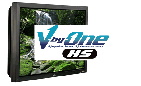
DisplayPort Receiver IP
core |
|
DisplayPort
Receiver IP core
DisplayPort預示著一個在視訊連接上新的選擇。這是被產業龍頭(Intel,
DELL, Apple
etc)設計用來達成更低花費的直接驅動顯示器。DisplayPort不會被許可證和專利費用所阻礙。
-
Support for 1,2 & 4-lane
-
Support 1.62 & 2.7GB/s link rate
-
80B/10B Decoder
-
16-bit de-scrambler
-
6,8,10,12 & 16 bit color support
|
 |
|
|
|
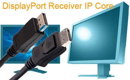
h.264 AVC Encoders from
Jointwave |
|
h.264 AVC
Encoders from Jointwave
從Jointwave而來的h.264
編碼器優秀的效能家族。
-
Input: Hsync Vsync 16bits parallel data, YUV4:2:2
-
Output: NAL standard packets
-
GOP configuration: I, IP
-
I16x16 and I4x4 all intra prediction modes
-
Multiple inter prediction modes
-
CABAC or CAVLC entropy encoding
-
Output bit rate: 0.5Mbps to 300Mbps
-
1/4 sub-pixel motion estimation
-
Mode Decision in 1/4 sub-pixel to get best quality
-
Hadmard transform for intra and inter prediction
-
Deblocking filter
-
External memory: SDRAM/DDR/DDR2
-
No external memory required for Intra Profile
|
 |
|
|
|
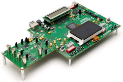
Cyclone III SDALTEVK Kit |
|
Cyclone III
SDALTEVK Kit
對於3G SDI 專業視訊發展器花費節約的工具組。
|
 |
|
|
|
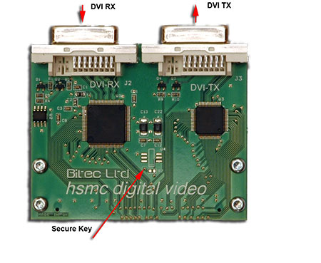
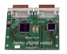
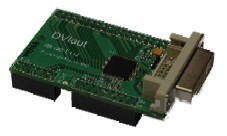
HSMC DUAL-LINK DVI Board |
|
HSMC DUAL-LINK
DVI Board
Two
channel Dual-Link DVI output board for Altera FPGA
development kits with HSMC expansion port.
-
Single link operation from 25-165 Megapixels per second
(VGA to UXGA)
-
Dual link operation up to 330 Megapixels per second
(3200×2400)
-
EDID reading/writing
-
12-bit (½ pixel) DDR input with flexible input clocking:
Single-clock/dual-edge or dual-clock/single-edge
-
I2C slave programming interface
-
Cable distance support: Over 10 m
-
Monitor detection through Hot-Plug
-
Compliant with DVI 1.0
|
 |
|
|
Alera
Cyclone III Development Kit |
| |
1.Cyclone III Video Development Kit(使用EP3C120F780主板和HSMC擴充子板) |
|
Cost effective kit targeted at
Video processing development using a Cyclone III device.
Cyclone III Video Development Kit :
-
Altera EP3C120F780 Development
board
-
HSMC Quad Video daughter
card
-
HSMC DVI daughter card
-
Collection of video reference
designs
|
 |
| |
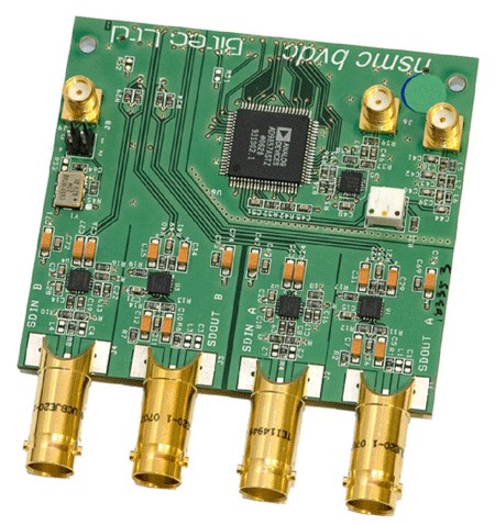
2.HSMC Broadcast Video Board |
|
Develop profesional video fpga
based systems using the Bitec BVDC.
HSMC Broadcast Video Board :
-
Dual ASI/SD-SDI
transmitter/receiver
-
Adaptive cable equalizers
-
Multi-rate cable drivers
-
27 Mhz VCXO
-
200Mhz Quadrature Modulating
14-bit DAC
-
Flexible clocking options for
DAC
|
 |
| |
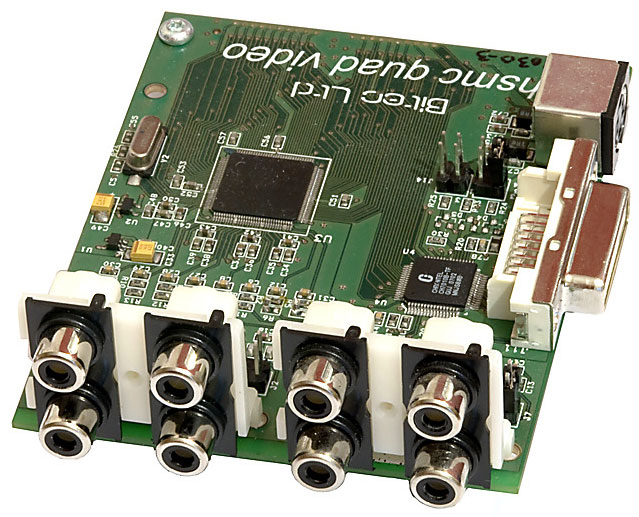
3.HSMC Quad Video Board |
|
Connect multiple live video
streams to your Altera FPGA using the Bitec Quad Video
board. Allows 4 S-Video or 8 Composite video inputs. An
integrated video output provides DVI, RGB or composite TV
connectivity.
HSMC Quad
Video Board :
-
Four Separate Video Decoder
Channels accept NTSC (M, 4.43), PAL (B, D, G, H, I, M, N),
and SECAM (B, D, G, K, K1, L)
-
Support ITU-R BT.601
-
High-Speed 9-Bit ADC on each
channel
-
Two Composite Inputs or One
S-video Input (for Each Channel)
-
Brightness, Contrast,
Saturation, Hue, and Sharpness Control Through i2c
-
Four Independent Polymorphic
Scalers
-
Standard Programmable Video
Input Format
-
ITU-R BT.656, 8-Bit 4:2:2 With
Embedded/Discrete Syncs
-
DVI Transmitter up to 165M
pixels/second
TV output supporting graphics resolutions up to 1024 x768
pixels
-
Support for all NTSC and PAL
formats on video output
-
Provides CVBS, S-Video and
SCART (RGB) outputs
|
 |
| |
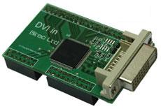
4.HSMC DVI Board |
|
Combined DVI input and output
board for Altera FPGA development kits with HSMC expansion
port.
HSMC DVI Board :
-
Digital Visual Interface
Compliant (DVI 1.0)
-
Supports resolutions from VGA
to UXGA (1600x1200 & 1920x1080)
-
25 - 165 Mhz Pixel rates
-
EDID data reading/writing
-
Monitor detection through
Hot-Plug
|
 |
| |
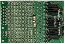
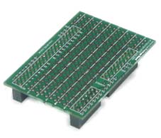
5.HSMC Prototyping board |
|
Prototyping board for Altera
FPGA development kits with HSMC expansion port.
HSMC
Prototyping board :
-
High quality, 4-layer, FR4 PCB
with plated thru holes
-
Convenient access points to
every pin on the HSMC connector
-
Plugs into Altera Stratix III
and Cyclone III development kits using the HSMC interface
standard
|
 |
| |
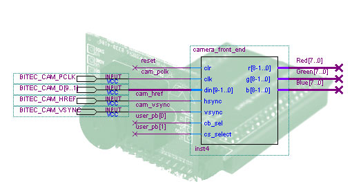
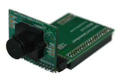
6.IP Camera Front End |
|
Altera optimised CMOS sensor
front end IP core.
IP Camera Front End :
-
Fully parameterised line
buffer·
-
Auto line length adaptation
for run-time resolution changes·
-
Minimal memory footprint·
-
Fully parameterised·
-
Bayer to RGB conversion·
-
Colour bar output·
-
Gamma correction/Colour space
conversion
|
 |
|
|
|
其它Altera原廠開發工具的Santa
Cruz介面相容 |
| |
1.SC Camera interface |
|
5.2 Mega pixel camera module for
the Altera FPGA development kits with Santa Cruz expansion
port.
-
5.2 Megapixel Omnivision CMOS
sensor
-
Resolution to 2,592x1,944
Nios II compatible
|
 |
| |
2.SC DVI input |
|
DVI input interface for Altera
FPGA development kits with Santa Cruz expansion port. Feed
real-time video into your FPGA designs!
-
Digital Visual Interface
Compliant (DVI 1.0)
-
Supports resolutions from VGA
to UXGA
-
25 – 165 Mhz Pixel rates
-
EDID data reading
-
Monitor detection through
Hot-Plug
|
 |
| |
3.SC DVI output |
|
DVI output interface for Altera
FPGA development kits with Santa Cruz expansion port.
-
Digital Visual Interface
Compliant (DVI 1.0)
-
Supports resolutions from VGA
to UXGA
-
25 – 165 Mhz Pixel rates
-
EDID data reading
-
Monitor detection through
Hot-Plug
|
 |
| |
4.SC Prototyping board |
|
Prototyping board for Altera
FPGA development kite with Santa Cruz expansion port.
-
4 Layer PCB with convenient
0.1" pitch spacing hole.
-
+3.3V, +5V and GND marked
access points
-
Fan-out of Santa Cruz
Connectors
|
 |
|
|
Altera DE3 |
|
Altera
DE3 最新多媒體平台
Altera Stratix III 3SL340 FPGA
with 338,000 LEs
DDR2 SO-DIMM Socket
SD Card Socket
Altera Serial Configuration
deivices (EPCS128) for Stratix III 3SL340
USB Blaster built-in for
programming and user API controlling
USB Host/Slave Controller with
one mini-AB for host/device and two type A for device
Eight 180-pin High Speed Terasic
Connectors ( HSTC )
Two 40-pin Expansion Headers
with diode protection
|
 |
|
|
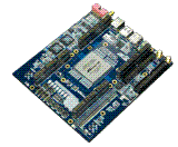
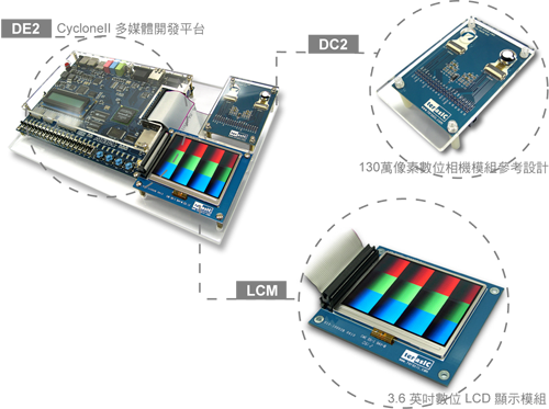
Altera DE2-70 多媒體平台及數位 LCD 面板和相機套件組 |
|
DE2-70多媒體數位平台榮獲 Altera美國總公司採購用於2006年四月全球嵌入式系統會議展出,並用於Altera
於全球大廠之多媒體應用展示, 本平台提供所有硬軟體及示範程式 (Verilog code)。 |
|
本套件包含:
|
 |
|
|
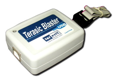
USB Blaster 下載 Cable |
|
|
 |
|
|
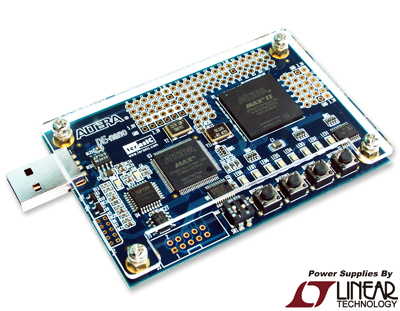
MAX II Micro Kit |
|
|
 |
|