|
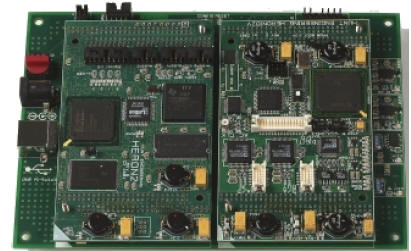
The RTG003 is
a self contained programmable system ideal for developing
Software Defined Radio. It can be used stand alone or
connected to a PC via the USB 2.0 connection.The fast A/D
and D/A channels are directly connected to the user
programmable FPGA, allowing data to be processed by a user
FPGA program.
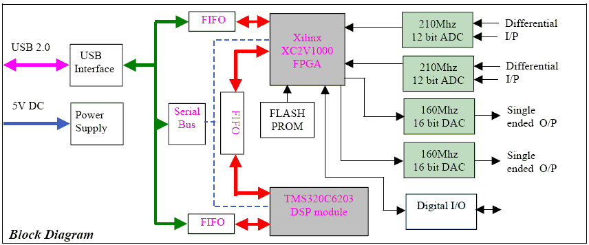
The FPGA can
be used to perform digital processing between the analogue
inputs and outputs, or the data can be passed to and from
the DSP or a PC using the USB 2.0 connection and provided
software.
The DSP can be programmed to perform whatever tasks you need
?the supplied example uses the FPGA to make a Digital Down
Conversion (DDC), the results of which are passed to the DSP
for protocol processing. The DSP then outputs its results to
the PC where a C++ program receives processes and graphs the
data.
Analogue I/P
2 channels with common or independent clocking set by jumper
Standard Input characteristics:
-
A/C coupled
50R, signal B/W from 750Hz to 500Mhz
-
Zero input
noise typically 3 levels maximum 8 levels
-
Offset
typically +-3 levels maximum +-12 levels
Optional Input types:
A/C coupled as standard but choose I/P impedance from
50R to 1K
D/C
D/C coupled choose I/P impedance from 50R to 1K, Signal
B/W 0hz to 500Mhz but each input must not exceed the
range 0v to +5V (of this module). This means a 4V DC
offset is required.
Zero input noise typically 3 levels maximum 8 levels
Offset typically +-12 levels maximum +-16 levels
Analogue O/P specifications
Standard
Output characteristics:
Optional Output types:
D/C coupled 10R, signal B/W 0 ?145Mhz
FPGA
Xilinx 1M gate Virtex-II FPGA, speed grade 4.
XC2V1000-4FG456
With no heatsink fitted (standard) the FPGA can
dissipate 2.4 Watts at 50deg C ambient temperature.
The power circuits are capable of delivering more than
this, so a heatsink may be required for your design.
If that is the case a larger 5V Power Supply Unit may
also be necessary
DSP
Texas Instruments 6203 @ 300Mhz, 32Mbytes sDRAM, 2
Mbytes Flash ROM
4 bit digital Outputs, 4 bit digital Inputs, 2 McBSPs
Host
Bus
USB 2.0 capable of up to 50Mbytes/second dependent on host
PC and USB configuration.
Maximum Dimensions :
160mm x 110mm x 21mm.
Power requirements
5V Max: 3.5A plus the power taken by the FPGA. Typ: 2.6A
plus FPGA
The Mains PSU included can supply up to 4A, which is enough
to power an FPGA
design that is less than the 2.4W bare package maximum
dissipation.
|